Fill Resistance: Seeing Where the Copper Actually Gets Hot
On a board like our LVSolarBuck, current has to get from one FET’s drain, across a copper pour, through a field of stitching vias, into another layer, and out through a different FET’s source pad. We have always known the pour needs to be wide and the via field dense enough. What we never had was a real number: how many milliohms that path costs, and where along it the copper runs hottest. KiCad, otherwise our full layout tool, has no built-in way to answer that. So we built the answer ourselves: Fill Resistance, a plugin we are publishing as open source at kicad-zone-resistance.
What it computes
Fill Resistance computes the DC resistance of a net’s copper, zone fills, traces and pads, between two sets of contacts, on a single layer or across several. Give it two terminals, a source FET pad and a sink FET pad, say, and it solves for how current actually distributes through the pour, reporting the resistance between them.
The output is more than a number: per-layer maps of potential and current density, a power density map, a raster overview of the mesh, per-via currents so you can check individual vias against their ampacity, and total dissipation at the chosen test current. PNGs, a summary.txt and a geometry_dump.json get saved under fill_res_results/<timestamp>/ next to the board file, so every run is a reproducible artifact you can go back to. There is also an experimental option to push the current-density heatmaps back into the open board as reference images on the spare User layers; it works, but the usability is not great yet, which is why it ships off by default.
How it works
Each copper layer is discretized as a finite-difference sheet, solved with a standard 5-point stencil, and the layers are coupled to each other through the net’s own via and through-hole-pad barrels (18 micron plating by default, configurable). It is not a generic field solver bolted onto KiCad; it is built around how copper pours and via fields actually behave.
The mesh is an adaptive 2:1-balanced quadtree by default: fine at copper boundaries, electrodes, traces and via mouths, coarsening to cells as large as 1 mm in the interior of a plane, roughly 8 million fine cells where a uniform grid would need about 2 million. A deferred-correction pass removes the flux bias the coarse-fine boundary would otherwise introduce, bringing the adaptive result within 0.03 percent of the uniform-grid answer. Traces narrower than three grid cells skip meshing entirely and are modeled as exact 1D resistor chains along their true centerline arc length, so thin traces carry no discretization error. Below 500,000 unknowns the solve is direct; above that it uses an AMG-preconditioned conjugate gradient solver (pyamg), falling back to Jacobi-CG where pyamg is unavailable, currently the case on ARM64 Linux. Same results, just slower.
Holes get real geometric attention rather than a shortcut: small vias below the 0.5 mm drill threshold are capped, larger ones open; populated through-hole pads model the full solder joint (lead, solder and barrel plating in parallel, a one-sided solder coat, the solder cone from a protruding lead); unpopulated pads model plating only; slots and ovals keep their true stadium shape. And because a real probe or bus bar sits somewhere between an ideal bonded connection and a conductor merely pressed on top, the plugin solves both bounding cases, equipotential (Dirichlet) and uniform injection, so the true resistance of any real contact falls between the two.
The pictures
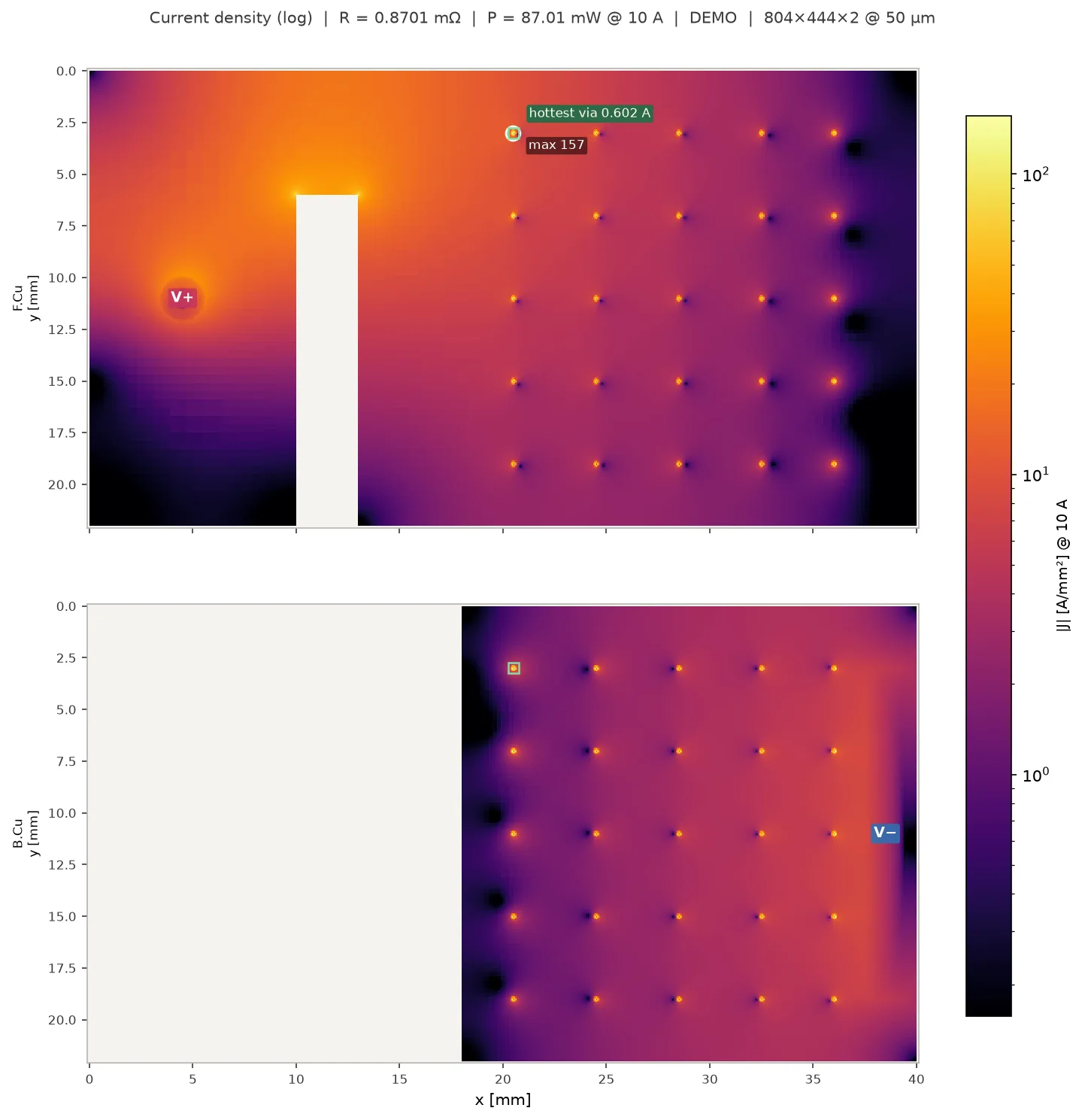 Current from a soldered THT-pad contact, injected at the drill-wall ring, squeezes past a notch in the
 F.Cu pour, transfers through the stitching-via field into the B.Cu pour, and leaves at the V- lug.
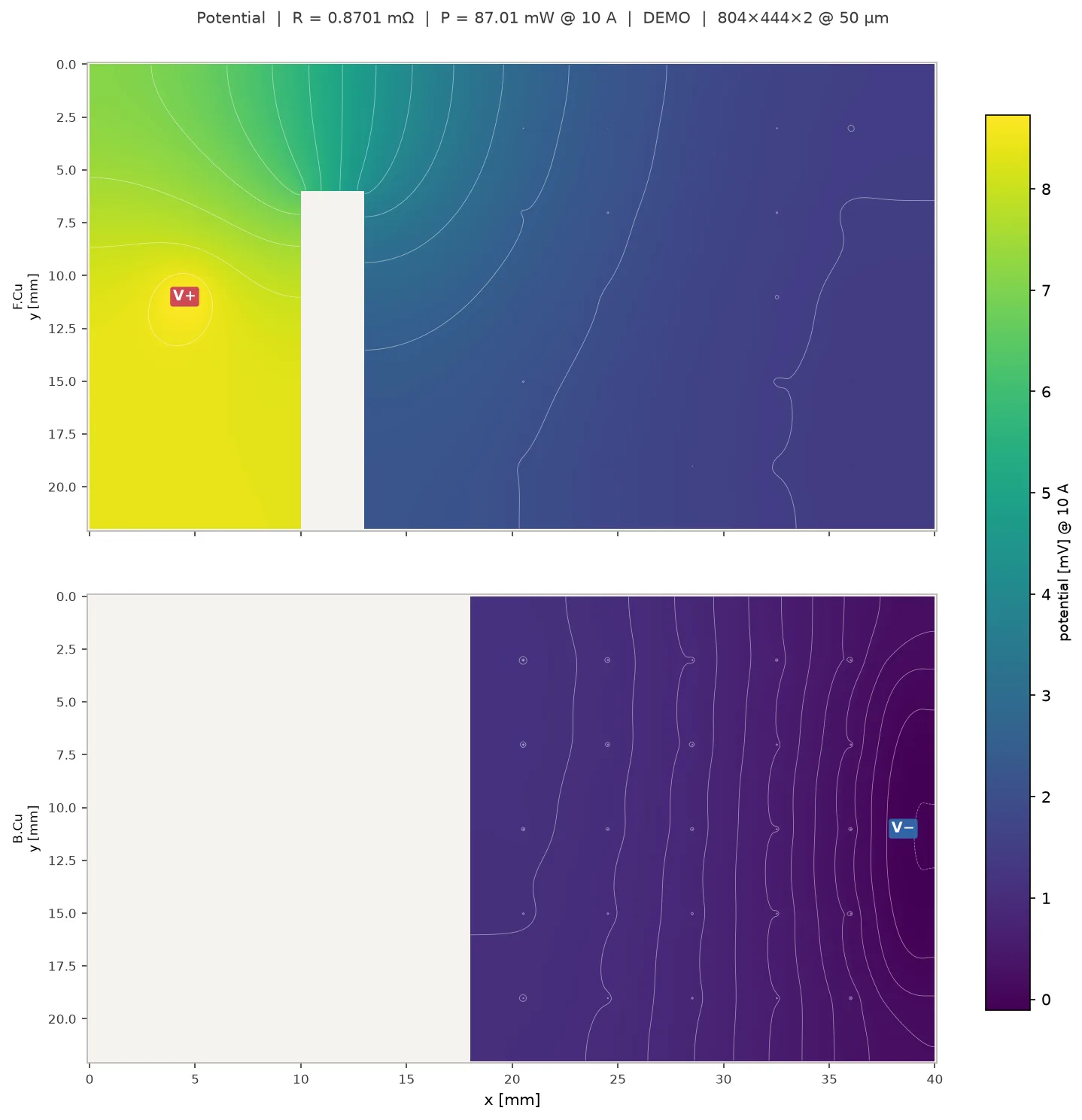 The contour lines bunch up where the field is strongest. Nearly the whole 8.7 mV drop happens right around the notch on
 F.Cu.
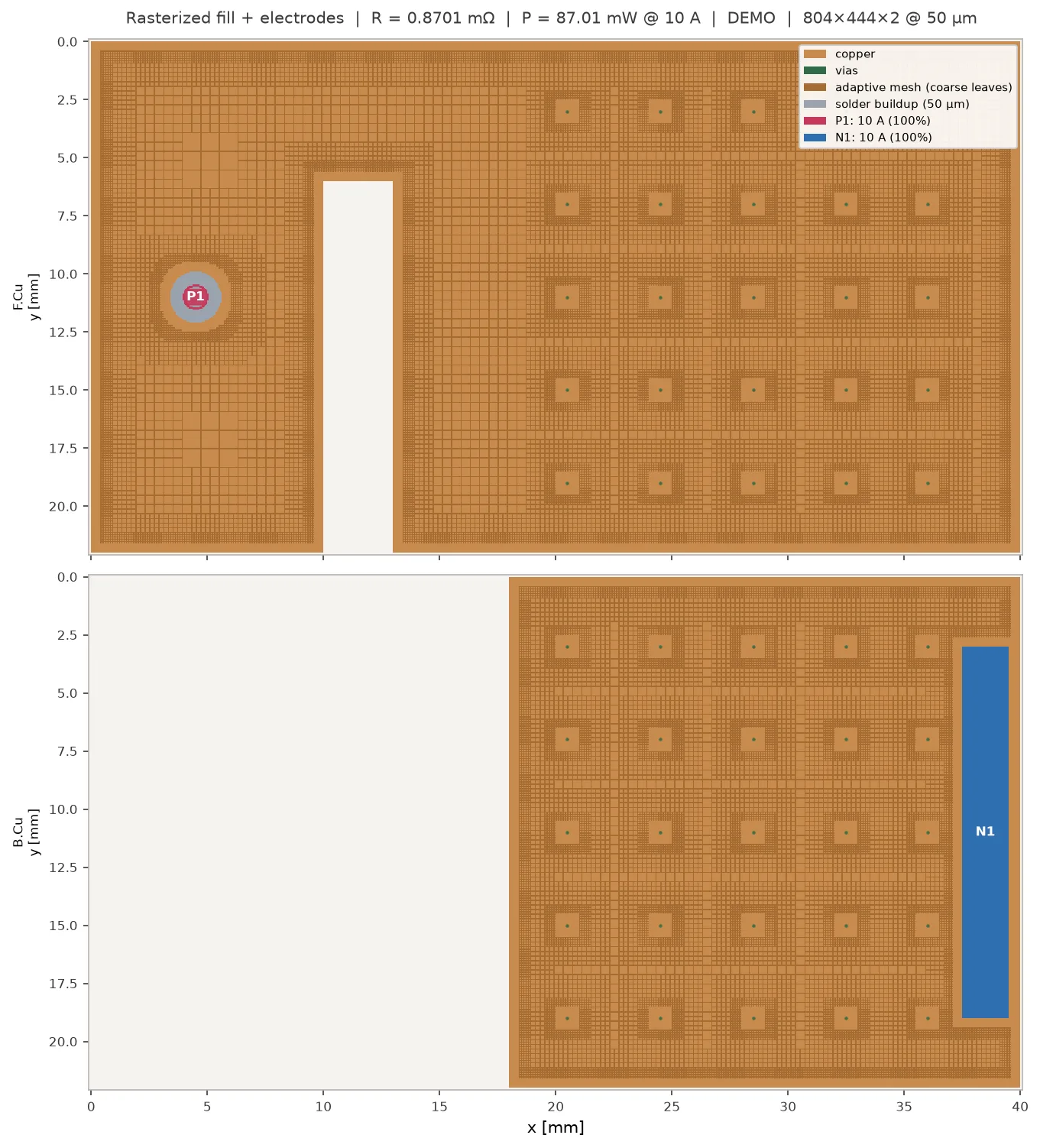 The adaptive mesh, the tin-gray solder coat on THT contact P1, and the via field, all in one view.
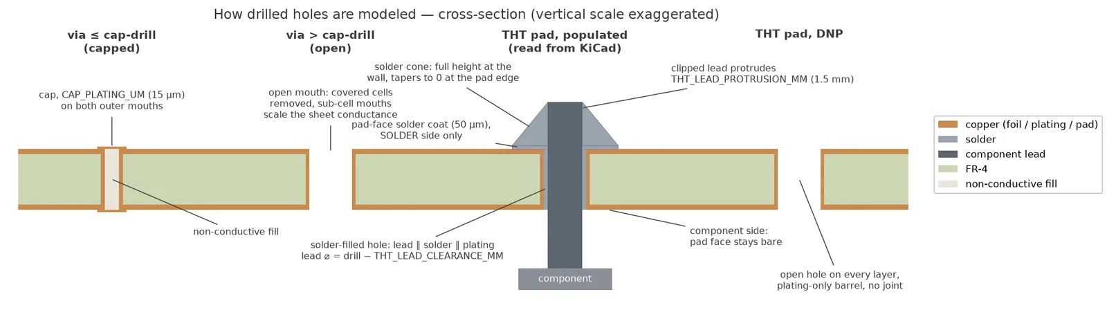 Capped small via, open large via, populated THT pad with its full solder joint, and a DNP THT pad.
What it is not
We want to be upfront about the limits, because they matter more than the pretty maps do. Fill Resistance solves DC resistance. It is not an AC impedance simulation: there is no inductance and no proximity effect anywhere in the model. The only AC effect it accounts for is skin effect, an optional correction at a user-set frequency using the exact 1D foil solution. Because the resistance-driven current distribution is the minimum-dissipation one, the skin-effect result at any frequency above zero is a rigorous lower bound on the real AC resistance, not an estimate of it. Rule of thumb: for 70 micron foil, skin effect is negligible below roughly 300 kHz and adds about 11 percent at 1 MHz. At the frequencies where inductive and proximity effects start to dominate, which can be a few kHz on a board with tight current loops, this tool will not tell you what is actually happening.
We pin the solver against exact analytic references (strip and annulus resistances, the acosh spreading resistance of two circular contacts on a sheet, skin-effect limits, power-balance identities) plus convergence and regression tests, so the arithmetic itself is trustworthy. Against real boards measured with a UT3513+ micro-ohm meter, computed values have come in within plus or minus 20 percent of measured, a gap we attribute to test-setup imperfections (probe placement, probe contact resistance versus our idealized contacts) and manufacturing tolerance on actual copper and plating thickness. The relative comparison between two layout variants is more trustworthy than any single absolute number.
Built with Claude, checked against hardware
We built Fill Resistance with Anthropic’s Claude (Claude Code, model Claude Fable 5), feature by feature, under our own direction and review; most commits carry a Co-Authored-By: Claude trailer. We say this openly because how a tool gets made matters, not just what it outputs. What keeps an LLM-assisted numerics project honest is the same thing that keeps a human-written one honest: an analytic test suite pinning the solver to known-correct answers, and hardware measurements checking the whole chain against a real micro-ohm meter on a real board.
Installing it
Fill Resistance is built on KiCad’s IPC API, not the deprecated SWIG API, so it needs KiCad 10.0.1 or newer with the API server enabled under Preferences, Plugins. Install the PCM addon zip from the releases page (Plugin and Content Manager, Install from File), or run it from source. On first load KiCad builds a private venv from requirements.txt (numpy, scipy, matplotlib, PySide6), and the Omega toolbar button appears once that finishes. To use it, mark V+ and V- injection terminals with rectangles on User.1 and User.2, or just select pads and vias, then hit the Omega button and pick net, layers, and test current. A typical real-board run finishes in about 8 seconds; large multi-layer pours at fine cell sizes can take minutes.
Windows is our development and test platform; Linux and macOS are audited but untested, and we would like to hear from anyone who tries them. It is GPL-3.0-or-later, same as the rest of our tooling.
| Resource | Link |
|---|---|
| Repository | git.b4l.co.th/B4L/kicad-zone-resistance |
| Forum thread | forum.kicad.info/t/resistance-plugin/70648 |
If you lay out high-current boards in KiCad and have ever eyeballed a pour width or a stitching via count, we would like to know what you find when you actually run the numbers on it.